4.2. How to generate mcs for FPGA
This chapter will introduce how to generate mcs file for Nuclei ddr200t development board.
After HBirdv2 E203 SoC is implemented on the FPGA subsystem of Nuclei ddr200t development board, we can develop embedded applications with it, just like with a real MCU chip.
Before starting the process of MCS generation, you should make sure that your environment is ready, which means e203_hbirdv2 project is ready in your working machine. About environmnet setting, please refer to Get ready.
Note
Nuclei ddr200t and mcu200t development boards could be used to support HBirdv2 E203 SoC development, here we just take Nuclei ddr200t development board as an example to introduce the development process. For Nuclei mcu200t development board, the development process is similar.
About the details of Nuclei ddr200t and mcu200t development boards, please refer to Nuclei Development Board.
About the connection between GPIO of HBirdv2 E203 SoC and peripherals of Nuclei ddr200t development board, please refer to HBirdv2 SoC GPIO Connection Table.
4.2.1. FPGA MCS generation
1. Prepare RTL
cd <your_e203_dir>/fpga

make install FPGA_NAME=ddr200t
Note
After running above commands, a folder named install will be created under <your_e203_dir>/fpga directory, and all RTL files needed to generate FPGA bitstream file are loacted in install/rtl folder.
2. Generate bit file
make bit FPGA_NAME=ddr200t
Note
Since the FPGA chip used in Nuclei ddr200t development board is Xilinx FPGA, so make sure that Vivado is installed in your machine before running above command.
3. Generate mcs file
make mcs FPGA_NAME=ddr200t
Note
If above steps run successfully, the FPGA MCS file will be generated under <your_e203_dir>/fpga/ddr200t/obj directory, named system.mcs.
4.2.2. FPGA MCS download
1. Hardware connenction
Connect Nuclei ddr200t development board and your computer with micro USB cable.
Connect power supply and turn on the power switch on Nuclei ddr200t development board.

Fig. 4.6 Connect with PC and power supply
2. Open Vivado, and select “Open Hardware Manager”
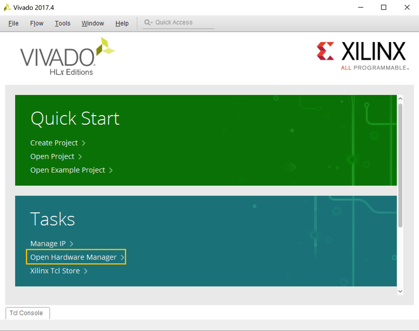
Fig. 4.7 Open Vivado Hardware Manager
3. Click “Auto Connect” button
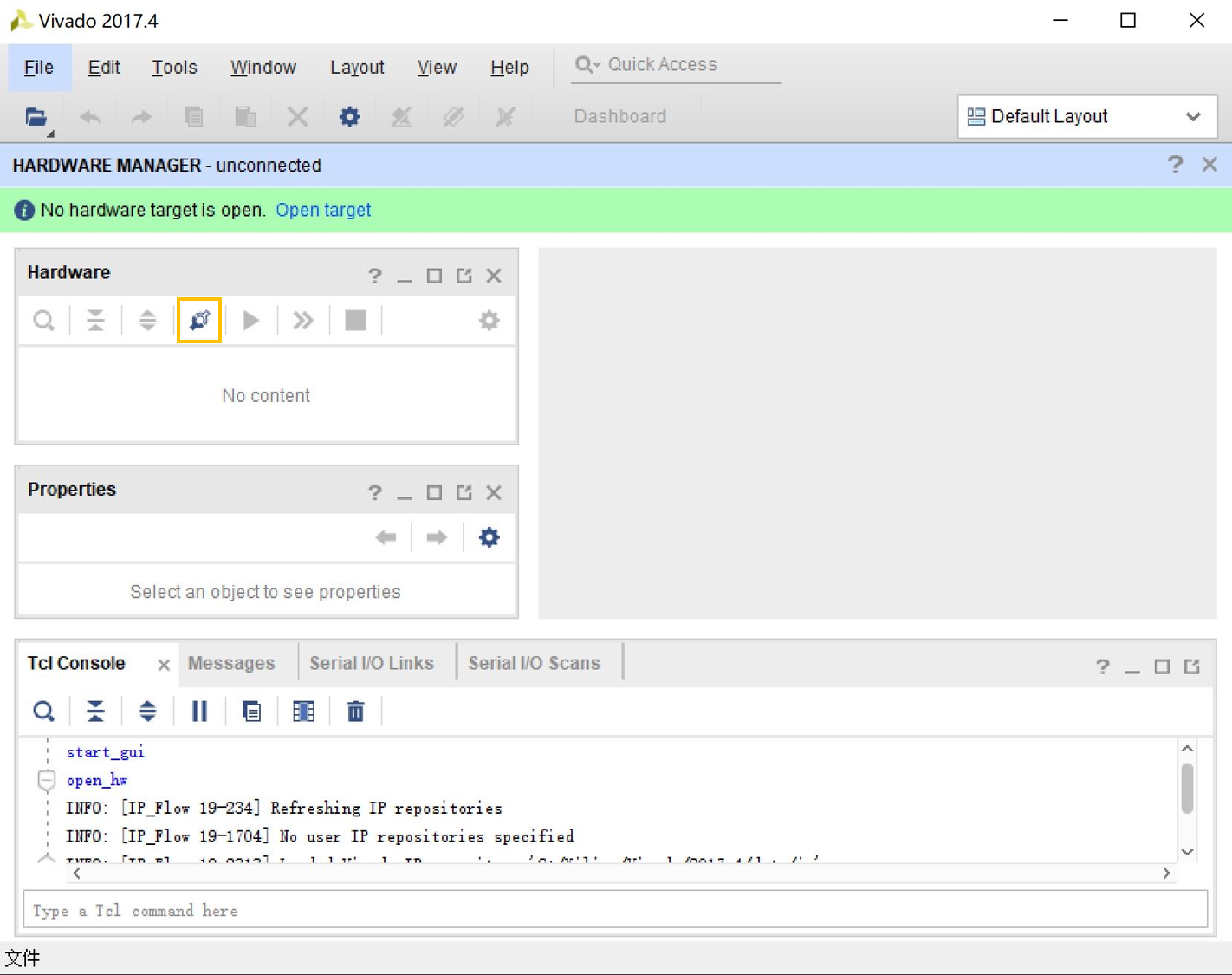
Fig. 4.8 Connect FPGA system on Nuclei ddr200t
4. Right-click on FPGA Device, and select “Add Configuration Memory Device”
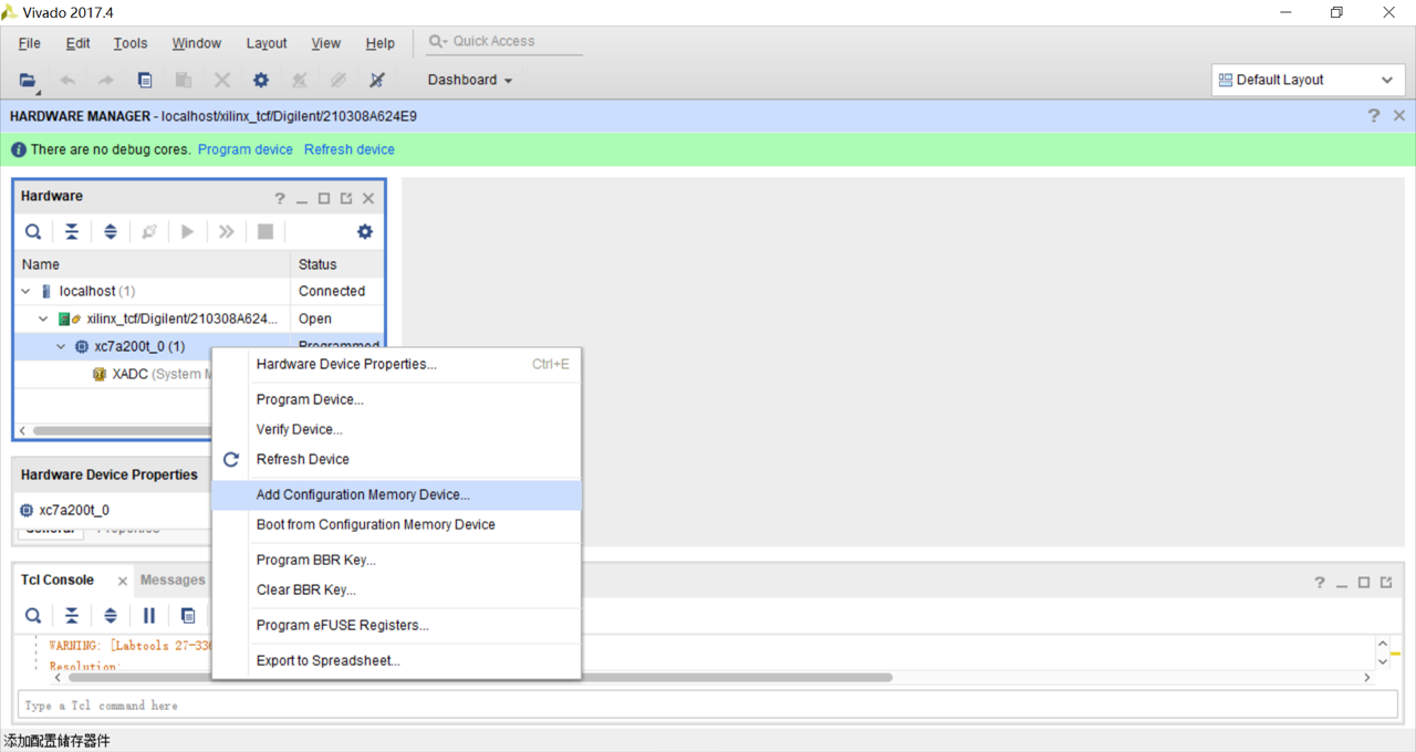
Fig. 4.9 Add Configuration Memory Device
5. Select Flash with following type
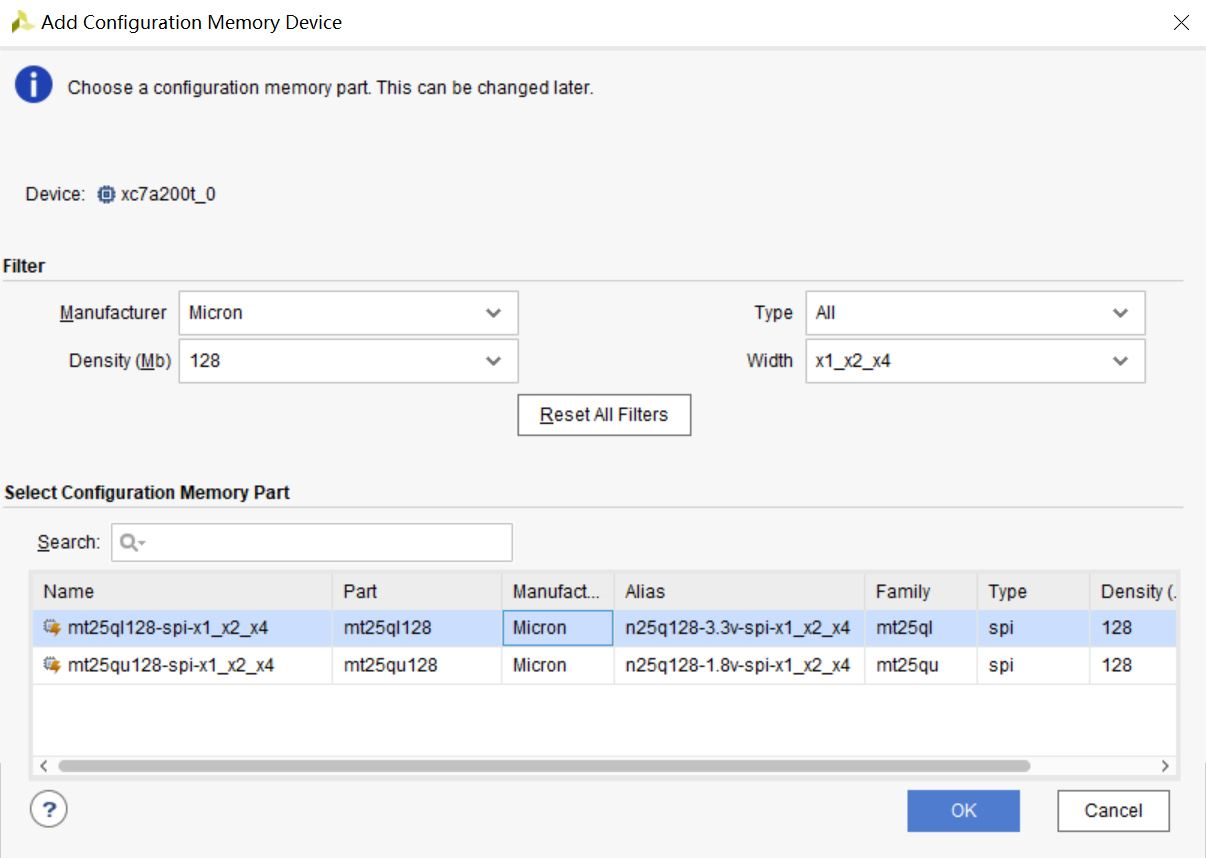
Fig. 4.10 Select Flash
Note
After completeing above steps, a dialog with info “Do you want to program the configuation memory device now?” will arise, then select “OK”.
6. Add <your_e203_dir>/fpga/ddr200t/obj/system.mcs as “Configuration file”, then click “OK”
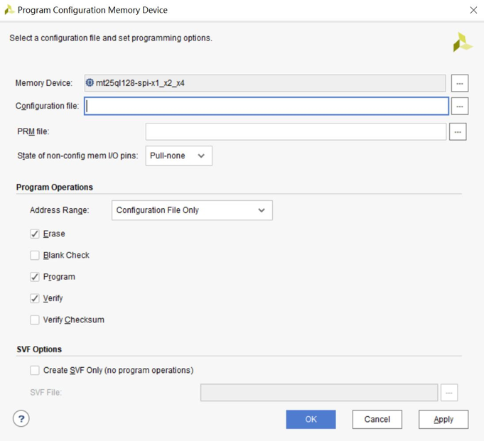
Fig. 4.11 Add MCS file
7. Downloading
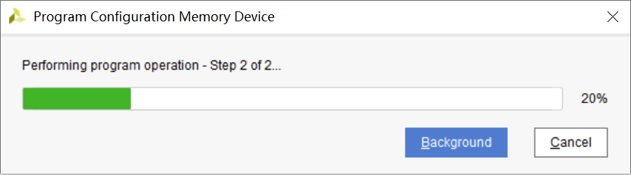
Fig. 4.12 Downloading
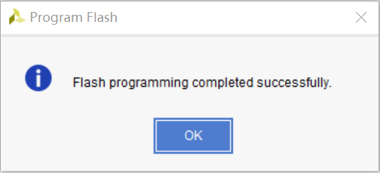
Fig. 4.13 Download successfully
Note
MCS file is downloaded to on-board nor flash, and each time Nuclei ddr200 development board is powered on, the bit stream will be loaded to FPGA from flash automatically.
4.2.3. Appendix
GPIOA Pad Num |
Peripheral/Interface |
GPIOB Pad Num |
Peripheral/Interface |
0 |
RGB LED26(R channel) |
0 |
J43(Pin1) |
1 |
RGB LED26(G channel) |
1 |
J43(Pin7) |
2 |
RGB LED26(B channel) |
2 |
J43(Pin2) |
3 |
BTN_UP |
3 |
J43(Pin8) |
4 |
BTN_DOWN |
4 |
J43(Pin3) |
5 |
BTN_LEFT |
5 |
J43(Pin9) |
6 |
BTN_RIGHT |
6 |
J43(Pin4) |
7 |
BTN_CENT |
7 |
J43(Pin10) |
8 |
LCD SPI(SCL) |
8 |
J44(Pin1) |
9 |
LCD SPI(CS) |
9 |
J44(Pin7) |
10 |
LCD SPI(SDI) |
10 |
J44(Pin2) |
11 |
LCD SPI(SDO) |
11 |
J44(Pin8) |
12 |
LCD RS |
12 |
J44(Pin3) |
13 |
LED21 |
13 |
J44(Pin9) |
14 |
EEPROM(U34) I2C(SCL) |
14 |
J44(Pin4) |
15 |
EEPROM(U34) I2C(SDA) |
15 |
J44(Pin10) |
16 |
J50 Pin8(MCU UART RX) |
16 |
J46(Pin1) |
17 |
J50 Pin2(MCU UART TX) |
17 |
J46(Pin7) |
18 |
LORA(U16) UART(TX) |
18 |
J46(Pin2) |
19 |
LORA(U16) UART(RX) |
19 |
J46(Pin8) |
20 |
LED0 |
20 |
J46(Pin3) |
21 |
LED1 |
21 |
J46(Pin9) |
22 |
LED2 |
22 |
J46(Pin4) |
23 |
LED3 |
23 |
J46(Pin10) |
24 |
LED4 |
24 |
J47(Pin1) |
25 |
LED5 |
25 |
J47(Pin7) |
26 |
SW0 |
26 |
J47(Pin2) |
27 |
SW1 |
27 |
J47(Pin8) |
28 |
SW2 |
28 |
J47(Pin3) |
29 |
SW3 |
29 |
J47(Pin9) |
30 |
SW4 |
30 |
J47(Pin4) |
31 |
SW5 |
31 |
J47(Pin10) |