3. Hummingbirdv2 SoC Peripherals
3.1. Overview
The peripherals in Hummingbirdv2 SoC are all listed in the table below.
Types |
Peripherals |
Nums |
Interrupt Ctrl |
CLINT |
1 |
PLIC |
1 |
|
Clk Ctrl |
LCLKGEN |
1 |
HCLKGEN |
1 |
|
IO Ctrl |
GPIO |
2(A,B) |
Communication Interface |
(Q)SPI |
3 |
I2C |
2 |
|
UART |
3 |
|
PWM |
PWM |
1(16 outputs) |
Timer |
WDT |
1 |
RTC |
1 |
|
Timer(CLINT) |
1 |
|
Timer(PWM) |
4 |
|
Power Mgr |
PMU |
1 |
3.2. CLINT
CLINT, Core Local Interrupts Controller. It’s used to generate Timer interrupt and Software Interrupt in HBirdv2 SoC. The registers of CLINT module are listed in the table below.
Address |
Name |
Reset Value |
Description |
0x0200_0000 |
msip |
0x0 |
Generate Software Interrupt |
0x0200_4000 |
mtimecmp_lo |
0xFFFF_FFFF |
Reflect lower 32-bit value of Timer Comparator |
0x0200_4004 |
mtimecmp_hi |
0xFFFF_FFFF |
Reflect upper 32-bit value of Timer Comparator |
0x0200_BFF8 |
mtime_lo |
0x0 |
Reflect lower 32-bit value of Timer Counter |
0x0200_BFFF |
mtime_hi |
0x0 |
Reflect upper 32-bit value of Timer Counter |
3.2.1. Software Interrupt
The CLINT unit can be used to generate the software interrupt. The register msip is implemented in CLINT unit as shown in the table below, only the least significant bit of msip is an effective bit. This bit is used to generate the software interrupt directly.
The software generates the software interrupt by writing 1 to the msip register.
The software clears the software interrupt by writing 0 to the msip register.
Field |
Bits |
Permission |
Default Value |
Description |
Reserved |
31:1 |
Readable, Write ignored |
N/A |
Reserverd |
MSIP |
0 |
RW |
0 |
Used to generate the software interrupt |
3.2.2. Timer Interrupt
The CLINT unit can be used to generate the timer interrupt. The key points are as follows.
The CLINT unit implements a 64-bit register mtimecmp, which is composed of {mtimecmp_hi, mtimecmp_lo}. This register is used as the comparison value of the timer. If the value of mtime is greater than the value of mtimecmp, then a timer interrupt is generated.
The software can clear the timer interrupt by overwriting the value of mtimecmp or mtime (so that the value of mtimecmp is greater than the value of mtime).
3.3. PLIC
PLIC, Platform Level Interrupt Controller, is part of RISC-V standard privileged architecture specification. It’s used for multiple external interrupt sources management and arbitration in HBirdv2 SoC.
It could support a maximum of 1024 external interrupt sources. In HBirdv2 SoC, 16 external interrupt sources are connected to PLIC unit, as listed in the table below. For multiple external interrupt inputs, PLIC unit arbitrates them into one-bit signal, and sents to the processor core as Machine External Interrupt.
Interrupt Number |
Interrupt Source |
0 |
Reserved(no interrupt) |
1 |
wdogcmp |
2 |
rtccmp |
3 |
uart0 |
4 |
uart1 |
5 |
uart2 |
6 |
qspi0 |
7 |
qspi1 |
8 |
qspi2 |
9 |
pwm0 |
10 |
pwm1 |
11 |
pwm2 |
12 |
pwm3 |
13 |
i2c0 |
14 |
i2c1 |
15 |
gpioA |
16 |
gpioB |
The registers of PLIC module are listed in the table below.
Address |
Reset Value |
Description |
0x0C00_0004 |
0x0 |
Source 1 priority |
0x0C00_0008 |
0x0 |
Source 2 priority |
…… |
…… |
…… |
0x0C00_0FFC |
0x0 |
Source 1023 priority |
…… |
…… |
…… |
0x0C00_1000 |
0x0 |
Start of pending array(read-only) |
…… |
…… |
…… |
0x0C00_107C |
0x0 |
End of pending array(read-only) |
…… |
…… |
…… |
0x0C00_2000 |
0x0 |
Target 0 enables |
…… |
…… |
…… |
0x0C20_0000 |
0x0 |
Target 0 priority threshold |
0x0C20_0004 |
0x0 |
Target 0 claim/complete |
Note
PLIC could support multiple targets, as HBirdv2 Processor is a single core processor and only support machine mode, so only target 0 is used here. Namely, targer 0 is HBirdv2 Processor.
“Source 1 priority” ~ “Source 1023 priority” are used to setting priority for each interrupt source, and the effective bit of this register is 3-bit, which means, the number of supported priority levels is 8. If multiple interrupt sources are set to same priority, then the interrupt with lowest ID has the the highest priority.
“Start of pending array” ~ “End of pending array” are used to indicate the pending status for each interrupt source, organized as 32 words of 32-bit. The pending bit for interrupt ID N is stored in bit (N mod 32) of word (N/32). Bit 0 of word 0, which represents the non-existent interrupt source 0, is always hardwired to zero.
“Target 0 enables” are used to setting interrupt enable for each interrupt source. The enables for a target are accessed as a contiguous array of 32 words, packed the same way as the pending bits. Bit 0 of enable word 0 represents the non-existent interrupt source 0 and is hardwired to 0.
“Target 0 priority threshold” is used to setting the threshold for a pending interrupt priority, and the effective bit of this register is 3-bit, the same as interrupt source priority register.
“Target 0 claim/complete” is actually two registers, claim register (read-only) and complete register (write-only). Each target can perform a claim by reading the claim/complete register, which returns the ID of the highest priority pending interrupt or zero if there is no pending interrupt for the target. A successful claim will also atomically clear the corresponding pending bit on the interrupt source. A target signals it has completed running a handler by writing the interrupt ID it received from the claim to the claim/complete register. This is routed to the corresponding interrupt gateway, which can now send another interrupt request to the PLIC.
3.4. LCLKGEN
LCLKGEN, Low-Speed Clock Generation, is used to generate clock for Always-On Domain in HBirdv2 SoC.
In the implementation of HBirdv2 FPGA prototype, LCLKGEN is an empty module. The clk for Always-On Domain is from 32.768KHz onboard crystal oscillator.
3.5. HCLKGEN
HCLKGEN, High-Speed Clock Generation, is used to generate clock for Main Domain in HBirdv2 SoC.
In the implementation of HBirdv2 FPGA prototype, HCLKGEN is an empty module. The clk for Main Domain is from Xilinx FPGA MMCM (Mixed-Mode Clock Manager), and the frequency is set to 16MHz.
3.6. GPIO
GPIO, General Purpose Input/Output, features are listed as below.
HBirdv2 SoC contains two GPIO modules, each has a group of 32 I/Os.
Each GPIO pin can be configured to work on SW control mode or IOF control mode.
Each GPIO pin can generate interrupt.
The registers of GPIO module are listed in the table below.
Register Name |
Offset Address |
Reset Value |
Description |
GPIO_PADDIR |
0x00 |
0x0 |
Pin direction (input or output) |
GPIO_PADIN |
0x04 |
0x0 |
Input value |
GPIO_PADOUT |
0x08 |
0x0 |
Output value |
GPIO_INTEN |
0x0C |
0x0 |
Interrupt enable |
GPIO_INTTYPE0 |
0x10 |
0x0 |
Interrupt type setting |
GPIO_INTTYPE1 |
0x14 |
0x0 |
Interrupt type setting |
GPIO_INTSTATUS |
0x18 |
0x0 |
Interrupt status |
GPIO_IOFCFG |
0x1C |
0x0 |
IOF configuration |
Note
GPIOA base address is 0x1001_2000, GPIOB base address is 0x1004_0000.
All GPIO registers are 32-bit, each bit corresponds to a GPIO pin.
3.6.1. SW or IOF Configuration
Each GPIO can be configured to work on SW control mode or IOF control mode.
SW Control Mode
When the corresponding bit of GPIO_IOFCFG register is set to 0, the GPIO pin works on SW control mode, which means normal GPIO mode, can be configurated as input (corresponding bit of GPIO_IOFCFG register set to 0) or output (corresponding bit of GPIO_IOFCFG register set to 1).
IOF Control Mode
When the corresponding bit of GPIO_IOFCFG register is set to 1, the GPIO pin works on IOF control mode, which means working as peripheral interface. In this working mode, the pin direction don’t need to set. The IOF map of GPIOA and GPIOB is listed in the table below.
GPIOA Pad Number |
IOF |
GPIOB Pad Number |
IOF |
0 |
PWM0_0 |
0 |
PWM2_0 |
1 |
PWM0_1 |
1 |
PWM2_1 |
2 |
PWM0_2 |
2 |
PWM2_2 |
3 |
PWM0_3 |
3 |
PWM2_3 |
4 |
PWM1_0 |
4 |
PWM3_0 |
5 |
PWM1_1 |
5 |
PWM3_1 |
6 |
PWM1_2 |
6 |
PWM3_2 |
7 |
PWM1_3 |
7 |
PWM3_3 |
8 |
QSPI1: SCK |
8 |
QSPI2: SCK |
9 |
QSPI1: CS |
9 |
QSPI2: CS |
10 |
QSPI1: DQ0 |
10 |
QSPI2: DQ0 |
11 |
QSPI1: DQ1 |
11 |
QSPI2: DQ1 |
12 |
QSPI1: DQ2 |
12 |
QSPI2: DQ2 |
13 |
QSPI1: DQ3 |
13 |
QSPI2: DQ3 |
14 |
I2C0: SCL |
14 |
I2C1: SCL |
15 |
I2C0: SDA |
15 |
I2C1: SDA |
16 |
UART0: RX |
16 |
UART1: RX |
17 |
UART0: TX |
17 |
UART1: TX |
18 |
UART2: RX |
18 |
- |
19 |
UART2: TX |
19 |
- |
20 |
- |
20 |
- |
21 |
- |
21 |
- |
22 |
- |
22 |
- |
23 |
- |
23 |
- |
24 |
- |
24 |
- |
25 |
- |
25 |
- |
26 |
- |
26 |
- |
27 |
- |
27 |
- |
28 |
- |
28 |
- |
29 |
- |
29 |
- |
30 |
- |
30 |
- |
31 |
- |
31 |
- |
3.6.2. GPIO Interrupt
GPIO interrupt type can be set through GPIO_INTTYPE0 and GPIO_INTTYPE1 registers. There are four triggers available.
INTTYPE0 = 0, INTTYPE1 = 0, Level 1
INTTYPE0 = 1, INTTYPE1 = 0, Level 0
INTTYPE0 = 0, INTTYPE1 = 1, Rise
INTTYPE0 = 1, INTTYPE1 = 1, Fall
When the GPIO pin interrupt is enabled (corresponding bit of GPIO_INTEN register set to 1), and configured interrupt type is detected, the GPIO interrupt will be generated, and the corresponding bit of GPIO_INTSTATUS register will be set. GPIO_INTSTATUS register could be cleared by reading its value.
Note
All 32 GPIO pins could generate interrupt, these 32 interrupt signals will exectue “OR” operation to generate a final interrupt signal, and sent to PLIC module as GPIO interrupt source. The specific interrupt source ID can be get by the value of GPIO_INTSTATUS register.
3.7. SPI
SPI, Serial Peripheral Interface, features are listed as below.
HBirdv2 SoC contains three SPI modules, QSPI0, QSPI1 and QSPI2.
QSPI0 is a special one, it could support SPI flash XiP (Execution in Place) mode. Namely, this QSPI controller implements a SPI flash sequencer, which exposes the external SPI flash contents as a read/execute-only memory-mapped device. In HBirdv2 SoC, QSPI0 is the interface dedicated to accessing external flash.
QSPI1 and QSPI2, these two modules have the same function, can be configured to work in single-SPI mode or quad-SPI mode, but don’t support SPI flash Xip mode. This QSPI module has transmit and receive FIFO buffer, and supports software programmable threshold setting to genenrate interrupt.
The registers of QSPI0 module are listed in the table below.
Register Name |
Offset Address |
Description |
SPI_SCKDIV |
0x00 |
Serial clock divisor |
SPI_SCKMODE |
0x04 |
Serial clock mode |
SPI_CSID |
0x10 |
Chip select ID |
SPI_CSDEF |
0x14 |
Chip select default |
SPI_CSMODE |
0x18 |
Chip select mode |
SPI_DELAY0 |
0x28 |
Delay control 0 |
SPI_DELAY1 |
0x2C |
Delay control 1 |
SPI_FMT |
0x40 |
Frame format |
SPI_TXDATA |
0x48 |
TX FIFO data |
SPI_RXDATA |
0x4C |
RX FIFO data |
SPI_TXMARK |
0x50 |
TX FIFO watermark |
SPI_RXMARK |
0x54 |
RX FIFO watermark |
SPI_FCTRL |
0x60 |
SPI flash interface control |
SPI_FFMT |
0x64 |
SPI flash instruction format |
SPI_IE |
0x70 |
SPI interrupt enable |
SPI_IP |
0x74 |
SPI interrupt pending |
Note
QSPI0 base address is 0x1001_4000.
All QSPI registers are 32-bit.
The registers of QSPI1 and QPSI2 module are listed in the table below.
Register Name |
Offset Address |
Description |
SPI_STATUS |
0x00 |
Status and control register |
SPI_CLKDIV |
0x04 |
Clock divider |
SPI_CMD |
0x08 |
SPI command |
SPI_ADR |
0x0C |
SPI address |
SPI_LEN |
0x10 |
SPI transfer length |
SPI_DUM |
0x14 |
SPI dummy cycles |
SPI_TXFIFO |
0x18 |
Transmit FIFO |
SPI_RXFIFO |
0x20 |
Receive FIFO |
SPI_INTCFG |
0x24 |
Interrupt configuration |
SPI_INTSTA |
0x28 |
Interrupt status |
Note
QSPI1 base address is 0x1002_4000, QSPI2 base address is 0x1003_4000.
All QSPI registers are 32-bit.
3.7.1. QPSI0 Registers
3.7.1.1. SPI_SCKDIV
Field |
Bit |
Attribute |
Reset Value |
Description |
Div |
11:0 |
RW |
0x3 |
The divisor used for generating SCK |
Note
Freq_SCK = Freq_SPI / (2*(Div+1))
Freq_SPI is the clock frequency of SPI module.
3.7.1.2. SPI_SCKMOD
Field |
Bit |
Attribute |
Reset Value |
Description |
pol |
1 |
RW |
0x0 |
Clock polarity |
0: inactive state of SCK is logical 0 |
||||
1: inactive state of SCK is logical 1 |
||||
pha |
0 |
RW |
0x0 |
Clock phase |
0: Data is sampled on the leading edge of SCK and shifted on the trailing edge of SCK |
||||
1: Data is shifted on the leading edge of SCK and sampled on the trailing edge of SCK |
3.7.1.3. SPI_CSID
Field |
Bit |
Attribute |
Reset Value |
Description |
csid |
31:0 |
RW |
0x0 |
Index of CS pin |
3.7.1.4. SPI_CSDEF
Field |
Bit |
Attribute |
Reset Value |
Description |
csdef |
31:0 |
RW |
0xFFFF |
Inactive state (polarity) of CS pins |
3.7.1.5. SPI_CSMODE
Field |
Bit |
Attribute |
Reset Value |
Description |
mode |
1:0 |
RW |
0x0 |
CS behavior |
0: AUTO, Assert/de-assert CS at the beginning/end of each frame |
||||
2: HOLD, Keep CS continuously asserted after the initial frame |
||||
3: OFF, Disable hardware control of the CS pin |
Note
In HOLD mode, the CS pin is de-asserted only when one of the following conditions occur.
A different value is written to csmode or csid.
A write to csdef changes the state of the selected pin.
Direct-mapped flash mode is enabled.
3.7.1.6. SPI_DELAY0
Field |
Bit |
Attribute |
Reset Value |
Description |
sckcs |
23:16 |
RW |
0x01 |
The delay between the last trailing edge of SCK and the de-assertion of CS |
When sckmode.pha = 1, an additional half-period delay is implicit |
||||
cssck |
7:0 |
RW |
0x01 |
The delay between the assertion of CS and the first leading edge of SCK |
When sckmode.pha = 0, an additional half-period delay is implicit |
3.7.1.7. SPI_DELAY1
Field |
Bit |
Attribute |
Reset Value |
Description |
interxfr |
23:16 |
RW |
0x00 |
The delay between two consecutive frames without de-asserting CS |
This ia applicable only when sckmode is HOLD or OFF |
||||
intercs |
7:0 |
RW |
0x01 |
The minimum CS inactive time between de-assertion and assertion |
3.7.1.8. SPI_FCTRL
Field |
Bit |
Attribute |
Reset Value |
Description |
en |
0 |
RW |
0x1 |
1: SPI flash XiP mode |
0: normal mode |
3.7.1.9. SPI_FFMT
Field |
Bit |
Attribute |
Reset Value |
Description |
pad_code |
31:24 |
RW |
0x00 |
First 8-bit to transmit during dummy cycles |
cmd_code |
23:16 |
RW |
0x03 |
Value of command byte |
data_proto |
13:12 |
RW |
0x0 |
Protocol for receiving data bytes |
addr_proto |
11:10 |
RW |
0x0 |
Protocol for transmitting address and padding |
cmd_proto |
9:8 |
RW |
0x0 |
Protocol for transmitting command |
pad_cnt |
7:4 |
RW |
0x0 |
Number of dummy cycles |
addr_len |
3:1 |
RW |
0x3 |
Number of address bytes(0 to 4) |
cmd_en |
0 |
RW |
0x1 |
Enable sending of command |
3.7.1.10. SPI_FMT
Field |
Bit |
Attribute |
Reset Value |
Description |
len |
19:16 |
RW |
0x8 |
The number of bits per frame(0 to 8) |
dir |
3 |
RW |
0x0 |
0: RX |
1: TX |
||||
endian |
2 |
RW |
0x0 |
0: Transmit MSB(most-significant bit) first |
1: Transmit LSB(least-significant bit) first |
||||
proto |
1:0 |
RW |
0x0 |
0: Single, DQ0(MOSI), DQ1(MISO) |
1: Dual, DQ0, DQ1 |
||||
2: Quad, DQ0, DQ1, DQ2, DQ3 |
3.7.1.11. SPI_TXDATA
Field |
Bit |
Attribute |
Reset Value |
Description |
full |
31 |
RO |
0x0 |
Indicate whether the transmit FIFO is ready to accept new entries |
data |
7:0 |
WO |
0x00 |
When full = 0, written data will be send to transmit FIFO |
When full = 1, written data will be ignored |
3.7.1.12. SPI_RXDATA
Field |
Bit |
Attribute |
Reset Value |
Description |
empty |
31 |
RO |
0x0 |
Indicate whether the receive FIFO contains new entries to be read |
data |
7:0 |
RO |
0x00 |
When empty = 0, data contains a valid frame |
When empty = 1, data doesn’t contain a valid frame |
3.7.1.13. SPI_TXMARK
Field |
Bit |
Attribute |
Reset Value |
Description |
txmark |
2:0 |
RW |
0x0 |
Specify the threshold at which the TX FIFO watermark interrupt triggers |
3.7.1.14. SPI_RXMARK
Field |
Bit |
Attribute |
Reset Value |
Description |
rxmark |
2:0 |
RW |
0x0 |
Specify the threshold at which the RX FIFO watermark interrupt triggers |
3.7.2. QPSI1(QSPI2) Registers
3.7.2.1. SPI_STATUS
SPI_STATUS register is actually two registers, ctrl register(write-only) and stat register(read-only).
Field |
Bit |
Attribute |
Reset Value |
Description |
CS |
11:8 |
WO |
- |
Chip select enable As QSPI1 and QSPI1 in HBirdv2 SoC only have one chip select signal, so set this field to 1, the CS signal could be enabled |
SRST |
4 |
WO |
- |
SW reset(clear FIFO) |
QWR |
3 |
WO |
- |
Quad-SPI Write |
QRD |
2 |
WO |
- |
Quad-SPI Read |
WR |
1 |
WO |
- |
Single-SPI Write |
RD |
0 |
WO |
- |
Single-SPI Read |
Field |
Bit |
Attribute |
Reset Value |
Description |
TXELEMS |
28:24 |
RO |
0 |
Number of elements in TX FIFO |
RXELEMS |
20:16 |
RO |
0 |
Number of elements in RX FIFO |
STATUS |
6:0 |
RO |
1 |
1: IDLE |
2: CMD |
||||
4: ADDR |
||||
16: DUMMY |
||||
32: DATA_TX |
||||
64: DATA_RX |
3.7.2.2. SPI_CLKDIV
Field |
Bit |
Attribute |
Reset Value |
Description |
CLKDIV |
7:0 |
RW |
0 |
The divisor used for generating SCK |
Note
Freq_SCK = Freq_SPI / (2*(CLKDIV+1))
Freq_SPI is the clock frequency of SPI module.
3.7.2.3. SPI_CMD
Field |
Bit |
Attribute |
Reset Value |
Description |
SPICMD |
31:0 |
RW |
0 |
Value of SPI command |
3.7.2.4. SPI_ADR
Field |
Bit |
Attribute |
Reset Value |
Description |
SPIADR |
31:0 |
RW |
0 |
Value of SPI address |
3.7.2.5. SPI_LEN
Field |
Bit |
Attribute |
Reset Value |
Description |
DATALEN |
31:16 |
RW |
0 |
Number of bits read or written |
ADDRLEN |
13:8 |
RW |
0 |
Number of bits of SPI address that should be sent |
CMDLEN |
5:0 |
RW |
0 |
Number of bits of SPI command that should be sent |
3.7.2.6. SPI_DUM
Field |
Bit |
Attribute |
Reset Value |
Description |
DUMMYWR |
31:16 |
RW |
0 |
Dummy cycles(nothing being written or read) between sending SPI command + SPI address and written data |
DUMMYRD |
15:0 |
RW |
0 |
Dummy cycles(nothing being written or read) between sending SPI command + SPI address and read data |
3.7.2.7. SPI_TXFIFO
Field |
Bit |
Attribute |
Reset Value |
Description |
TX |
31:0 |
RW |
0 |
Write data into TX FIFO |
3.7.2.8. SPI_RXFIFO
Field |
Bit |
Attribute |
Reset Value |
Description |
RX |
31:0 |
RW |
0 |
Read data from RX FIFO |
3.7.2.9. SPI_INTCFG
Field |
Bit |
Attribute |
Reset Value |
Description |
EN |
31 |
RW |
0 |
1: enable SPI interrupt |
0: disable SPI interrupt |
||||
RXTH |
12:8 |
RW |
0 |
Specify the threshold at which the RX FIFO watermark interrupt triggers |
TXTH |
4:0 |
RW |
0 |
Specify the threshold at which the TX FIFO watermark interrupt triggers |
3.8. I2C
I2C, Inter-Integrated Circuit, features are listed as below.
HBirdv2 SoC contains two I2C modules
Software-programmable SDL clock frequency
Supports interrupt generation
The registers of I2C module are listed in the table below.
Register Name |
Offset Address |
Description |
I2C_PRE |
0x00 |
Clock prescale register |
I2C_CTR |
0x04 |
Control register |
I2C_RX |
0x08 |
Receive register |
I2C_STATUS |
0x0C |
Status register |
I2C_TX |
0x10 |
Transmit register |
I2C_CMD |
0x14 |
Command register |
Note
I2C0 base address is 0x1002_5000, I2C1 base address is 0x1003_5000.
All I2C registers are 32-bit.
3.8.1. I2C Registers
3.8.1.1. I2C_PRE
Field |
Bit |
Attribute |
Reset Value |
Description |
PRE |
15:0 |
RW |
0 |
The prescale used for generating SCL clock |
Note
PRE = Freq_I2C / ((5*Freq_SCL) - 1)
Freq_I2C is the clock frequency of I2C module.
3.8.1.2. I2C_CTR
Field |
Bit |
Attribute |
Reset Value |
Description |
EN |
7 |
RW |
0 |
1: enable I2C 0: disable I2C |
IE |
6 |
RW |
0 |
1: enable I2C interrupt 0: disable I2C interrupt |
3.8.1.3. I2C_TX
Field |
Bit |
Attribute |
Reset Value |
Description |
TX |
7:0 |
RW |
0 |
Next byte to be transmitted |
3.8.1.4. I2C_RX
Field |
Bit |
Attribute |
Reset Value |
Description |
RX |
7:0 |
RW |
0 |
Last byte received |
3.8.1.5. I2C_CMD
Field |
Bit |
Attribute |
Reset Value |
Description |
STA |
7 |
RW |
0 |
Generate start condition |
STOP |
6 |
RW |
0 |
Generate stop condition |
RD |
5 |
RW |
0 |
Read from slave |
WR |
4 |
RW |
0 |
Write to slave |
ACK |
3 |
RW |
0 |
When a receiver, sent ACK(ACK=0) or NACK(ACK=1) |
IACK |
0 |
RW |
0 |
Interrupt acknowledge |
When set, clears a pending interrupt |
3.8.1.6. I2C_STATUS
Field |
Bit |
Attribute |
Reset Value |
Description |
RXA |
7 |
RO |
0 |
Received acknowledge from slave |
1: No acknowledge received |
||||
0: Acknowledge received |
||||
BUSY |
6 |
RO |
0 |
Indicate I2C bus busy |
1: START signal is detected |
||||
0: STOP signal is detected |
||||
AL |
5 |
RO |
0 |
Arbitration lost |
This bit is set when I2C lost arbitration |
||||
TIP |
1 |
RO |
0 |
Transfer in progress |
1: transferring data |
||||
0: transfer completed |
||||
IRQ |
0 |
RO |
0 |
This bit is set when an interrupt is pending |
3.9. UART
UART, Universal Asynchronous Receiver-Transmitter, features are listed as below.
HBirdv2 SoC contains three UART modules
Fully programmable serial interface characteristics
Even, odd or no-parity bit generation/detection
A data length can be 8 or 9 bits
1 or 2 stop bit generation
Software-programmable threshold setting to generate interrupt
The registers of UART module are listed in the table below.
Register Name |
Offset Address |
Description |
UART_RBR |
0x00 |
Receiver buffer register |
UART_DLL |
0x00 |
Divisor latch register(LSB) |
UART_THR |
0x00 |
Transmitter holding register |
UART_DLM |
0x04 |
Divisor latch register(MSB) |
UART_IER |
0x04 |
Interrupt enable register |
UART_IIR |
0x08 |
Interrupt identification register |
UART_FCR |
0x08 |
FIFO control register |
UART_LCR |
0x0C |
Line control register |
UART_LSR |
0x14 |
Line status register |
Note
UART0 base address is 0x1001_3000, UART1 base address is 0x1002_3000, UART2 base address is 0x1003_3000.
All UART registers are 32-bit.
UART_RBR is read-only register, UART_THR is write-only register, UART_DLL is readable and writable register, these three registers share the same access address. If access UART_DLL register, DLAB field of UART_LCR register should be set.
UART_IER is readable and writable register, UART_DLM is readable and writable register, these two registers share the same access address. If access UART_DLM register, DLAB field of UART_LCR register should be set.
UART_IIR is read-only register, UART_FCR is write-only register, these two registers share the same access address.
3.9.1. UART Registers
3.9.1.1. UART_DLL
Field |
Bit |
Attribute |
Reset Value |
Description |
DLL |
7:0 |
RW |
0 |
Least significant byte of the Baud rate generator counter |
Note
This register is only valid when DLAB field of UART_LCR register is set.
Baud_Rate = Freq_UART / ({DLM, DLL} + 1)
3.9.1.2. UART_DLM
Field |
Bit |
Attribute |
Reset Value |
Description |
DLM |
7:0 |
RW |
0 |
Most significant byte of the Baud rate generator counter |
Note
This register is only valid when DLAB field of UART_LCR register is set.
Baud_Rate = Freq_UART / ({DLM, DLL} + 1)
3.9.1.3. UART_RBR
Field |
Bit |
Attribute |
Reset Value |
Description |
RX |
7:0 |
RO |
0 |
Last received character |
3.9.1.4. UART_THR
Field |
Bit |
Attribute |
Reset Value |
Description |
TX |
7:0 |
WO |
- |
The character to be transmitted next |
3.9.1.5. UART_FCR
Field |
Bit |
Attribute |
Reset Value |
Description |
RX_TRG_LEVL |
7:6 |
WO |
- |
RX FIFO trigger level |
00: 1byte |
||||
01: 4bytes |
||||
10: 8bytes |
||||
11: 14bytes |
||||
TXFIFO_CLR |
2 |
WO |
- |
1: TX FIFO reset |
RXFIFO_CLR |
1 |
WO |
- |
1: RX FIFO reset |
3.9.1.6. UART_LCR
Field |
Bit |
Attribute |
Reset Value |
Description |
DLAB |
7 |
RW |
0 |
1: Allow access to UART_DLM, UART_DLL registers |
0: Allow access to UART_RBR, UART_THR, UART_IER registers |
||||
PS |
5:4 |
RW |
0 |
Parity select |
00: odd |
||||
01: even |
||||
10: space |
||||
11: mark |
||||
PEN |
3 |
RW |
0 |
Parity enable |
1: enable |
||||
0: disable |
||||
STB |
2 |
RW |
0 |
Number of stop bits |
0: 1 |
||||
1: 2 |
||||
WLS |
1:0 |
RW |
0 |
Word length select |
00: 5 bits/character |
||||
01: 6 bits/character |
||||
10: 7 bits/character |
||||
11: 8 bits/character |
3.9.1.7. UART_LSR
Field |
Bit |
Attribute |
Reset Value |
Description |
TEMT |
6 |
RO |
1 |
This bit is set when THR and TX FIFO are both empty |
THRE |
5 |
RO |
1 |
This bit is set when TX FIFO is empty |
PE |
2 |
RO |
0 |
This bit is set when parity error occurs |
DR |
0 |
RO |
0 |
This bit is set when incoming character has been received |
3.10. PWM
PWM, Pulse-Width Modulation. HBirdv2 SoC has one PWM module, which contains 4 Timer units. These four Timer units have the same functions, features are listed as below.
Each Timer unit have 4 output channel.
Configurable trigger input sources.
Configurable prescaler for each Timer.
Configurable counting mode for each Timer.
Interrupt generation (configurable interrupt source)
The registers of PWM module are listed in the table below.
Register Name |
Offset address |
Description |
TIMx_CMD(x=0,1,2,3) |
0x40*x + 0x00 |
Timerx command register |
TIMx_CFG(x=0,1,2,3) |
0x40*x + 0x04 |
Timerx configuration register |
TIMx_TH(x=0,1,2,3) |
0x40*x + 0x08 |
Timerx threshold configuration register |
TIMx_CH0_TH(x=0,1,2,3) |
0x40*x + 0x0C |
Timerx channel0 threshold configuration register |
TIMx_CH1_TH(x=0,1,2,3) |
0x40*x + 0x10 |
Timerx channel1 threshold configuration register |
TIMx_CH2_TH(x=0,1,2,3) |
0x40*x + 0x14 |
Timerx channel2 threshold configuration register |
TIMx_CH3_TH(x=0,1,2,3) |
0x40*x + 0x18 |
Timerx channel3 threshold configuration register |
TIMx_CNT(x=0,1,2,3) |
0x40*x + 0x2C |
Timerx counter register |
PWM_ENT_CFG |
0x100 |
PWM event configuration register |
PWM_CH_EN |
0x104 |
PWM channel enable register |
Note
PWM base address is 0x1001_5000.
PWM module contains 4 Timer units, TIMx(x=0,1,2,3) are the registers corresponding to Timer0, Timer1, Timer2, Timer3 respectively.
All PWM registers are 32-bit.
3.10.1. PWM Registers
3.10.1.1. TIMx_CMD
Field |
Bit |
Attribute |
Reset Value |
Description |
ARM |
4 |
WO |
0 |
Timerx arm command |
RESET |
3 |
WO |
0 |
Timerx reset command |
UPDATE |
2 |
WO |
0 |
Timerx update command |
STOP |
1 |
WO |
0 |
Timerx stop command |
START |
0 |
WO |
0 |
Timerx start command |
3.10.1.2. TIMx_CFG
Field |
Bit |
Attribute |
Reset Value |
Description |
PRESC |
23:16 |
RW |
0 |
Value of Timerx prescaler |
UPDOWNSEL |
12 |
RW |
0 |
Timerx count mode |
0: The counter counts up and down when reach threshold |
||||
1: The counter counts up and resets to 0 when reach threshold |
||||
CLKSEL |
11 |
RW |
0 |
Timerx clock source select |
0: High-speed clock from Main domain |
||||
1: Low-speed clock from Always-on domain |
||||
MODE |
10:8 |
RW |
0 |
Timerx work mode |
0: trigger event at each clock cycle |
||||
1: trigger event if input source is 0 |
||||
2: trigger event if input source is 1 |
||||
3: trigger event on input source rising edge |
||||
4: trigger event on input source falling edge |
||||
5: trigger event on input source falling or rising edge |
||||
6: trigger event on input source rising edge when ARM field of TIMx_CMD register is set |
||||
7: trigger event on input source falling edge when ARM field of TIMx_CMD register is set |
||||
INSEL |
7:0 |
RW |
0 |
Timerx input source select |
0~31: GPIOA[0] to GPIOA[31] |
||||
32~35: channel 0 to 3 of Timer0 |
||||
36~39: channel 0 to 3 of Timer1 |
||||
40~43: channel 0 to 3 of Timer2 |
||||
44~47: channel 0 to 3 of Timer3 |
3.10.1.3. TIMx_TH
Field |
Bit |
Attribute |
Reset Value |
Description |
TH_HI |
31:16 |
RW |
0 |
Counter end value |
TH_LO |
15:0 |
RW |
0 |
Counter start value |
3.10.1.4. TIMx_CH0_TH
Field |
Bit |
Attribute |
Reset Value |
Description |
MODE |
18:16 |
RW |
0 |
Timerx channel 0 output mode when threshold match |
0: set |
||||
1: toggle, and when next threshold match, output is clear |
||||
2: set, and when next threshold match, output is clear |
||||
3: toggle |
||||
4: clear |
||||
5: toggle, and when next threshold match, output is set |
||||
6: clear, and when next threshold match, output is set |
||||
TH |
15:0 |
RW |
0 |
Timerx channel 0 threshold |
3.10.1.5. TIMx_CH1_TH
Field |
Bit |
Attribute |
Reset Value |
Description |
MODE |
18:16 |
RW |
0 |
Timerx channel 1 output mode when threshold match |
0: set |
||||
1: toggle, and when next threshold match, output is clear |
||||
2: set, and when next threshold match, output is clear |
||||
3: toggle |
||||
4: clear |
||||
5: toggle, and when next threshold match, output is set |
||||
6: clear, and when next threshold match, output is set |
||||
TH |
15:0 |
RW |
0 |
Timerx channel 1 threshold |
3.10.1.6. TIMx_CH2_TH
Field |
Bit |
Attribute |
Reset Value |
Description |
MODE |
18:16 |
RW |
0 |
Timerx channel 2 output mode when threshold match |
0: set |
||||
1: toggle, and when next threshold match, output is clear |
||||
2: set, and when next threshold match, output is clear |
||||
3: toggle |
||||
4: clear |
||||
5: toggle, and when next threshold match, output is set |
||||
6: clear, and when next threshold match, output is set |
||||
TH |
15:0 |
RW |
0 |
Timerx channel 2 threshold |
3.10.1.7. TIMx_CH3_TH
Field |
Bit |
Attribute |
Reset Value |
Description |
MODE |
18:16 |
RW |
0 |
Timerx channel 3 output mode when threshold match |
0: set |
||||
1: toggle, and when next threshold match, output is clear |
||||
2: set, and when next threshold match, output is clear |
||||
3: toggle |
||||
4: clear |
||||
5: toggle, and when next threshold match, output is set |
||||
6: clear, and when next threshold match, output is set |
||||
TH |
15:0 |
RW |
0 |
Timerx channel 3 threshold |
3.10.1.8. TIMx_CNT
Field |
Bit |
Attribute |
Reset Value |
Description |
CNT |
15:0 |
RO |
0 |
Value of Timex counter |
3.10.1.9. PWM_ENT_CFG
Field |
Bit |
Attribute |
Reset Value |
Description |
ENA |
19:16 |
RW |
0 |
Interrupts enable |
ENA[i] = 1, enable PWM interrupt i (i=0,1,2,3) |
||||
ENA[i] = 0, disable PWM interrupt i (i=0,1,2,3) |
||||
SEL3 |
15:12 |
RW |
0 |
PWM interrupt 3 source select |
0: Timer0 channel 0 |
||||
1: Timer0 channel 1 |
||||
… |
||||
3: Timer0 channel 3 |
||||
4: Timer1 channel 0 |
||||
… |
||||
15: Timer3 channel 3 |
||||
SEL2 |
11:8 |
RW |
0 |
PWM interrupt 2 source select |
0: Timer0 channel 0 |
||||
1: Timer0 channel 1 |
||||
… |
||||
3: Timer0 channel 3 |
||||
4: Timer1 channel 0 |
||||
… |
||||
15: Timer3 channel 3 |
||||
SEL1 |
7:4 |
RW |
0 |
PWM interrupt 1 source select |
0: Timer0 channel 0 |
||||
1: Timer0 channel 1 |
||||
… |
||||
3: Timer0 channel 3 |
||||
4: Timer1 channel 0 |
||||
… |
||||
15: Timer3 channel 3 |
||||
SEL0 |
3:0 |
RW |
0 |
PWM interrupt 0 source select |
0: Timer0 channel 0 |
||||
1: Timer0 channel 1 |
||||
… |
||||
3: Timer0 channel 3 |
||||
4: Timer1 channel 0 |
||||
… |
||||
15: Timer3 channel 3 |
3.10.1.10. PWM_TIMER_EN
Field |
Bit |
Attribute |
Reset Value |
Description |
TIMER_EN |
3:0 |
RW |
0 |
Timers enable |
TIMER_EN[i] = 1, enable Timeri (i=0,1,2,3) |
||||
TIMER_EN[i] = 0, disable Timeri (i=0,1,2,3) |
Note
In the implementation of HBirdv2 FPGA prototype, this register is invalid, all Timer units are always enabled.
3.11. WDT
WDT, Watchdog Timer, features are listed as below.
HBirdv2 SoC contains one WDT module in Always-on Domain.
Programmable comparison threshold.
If the watchdog functionality is not required, WDT could be used as a programmable periodic interrupt source.
WDT registers can only be updated by presenting a WDT key sequence.
The registers of WDT module are listed in the table below.
Register Name |
Address |
Reset Value |
Description |
WDOGCFG |
0x1000_0000 |
0 |
Watchdog configuration register |
WDOGCOUNT |
0x1000_0008 |
0 |
Watchdog count register |
WDOGS |
0x1000_0010 |
0 |
Watchdog shadow register |
WDOGFEED |
0x1000_0018 |
0 |
Watchdog feed register |
WDOGKEY |
0x1000_001C |
0 |
Watchdog key register |
WDOGCMP |
0x1000_0020 |
0xFFFF |
Watchdog compare register |
Note
WDOGCFG, WDOGCOUNT, WDOGFEED and WDOGCMP registers are 32-bit.
WDOGS and WDOGCMP registers are 16-bit.
3.11.1. WDT Registers
3.11.1.1. WDOGCFG
Field |
Bit |
Attribute |
Reset Value |
Description |
wdogcmpip |
28 |
RW |
0 |
Interrupt pending bit |
wdogencoreawake |
13 |
RW |
0 |
If this bit is set, watchdog counter increments if the processor core is not asleep |
wdogenalways |
12 |
RW |
0 |
If this bit is set, watchdog counter always increments |
wdogzerocmp |
9 |
RW |
0 |
If this bit is set, watchdog counter reset to zero one cycle after comparison threshold match |
wdogrsten |
8 |
RW |
0 |
If this bit is set, watchdog could cause a full reset |
wdogscale |
3:0 |
RW |
0 |
Scale the watchdog counter value before feeding it to comparator |
3.11.1.2. WDOGCOUNT
Field |
Bit |
Attribute |
Reset Value |
Description |
wdogcnt |
30:0 |
RW |
0 |
Value of watchdog counter |
Note
Bit 31 of WDOGCOUNT returns a zero when read.
3.11.1.3. WDOGKEY
Field |
Bit |
Attribute |
Reset Value |
Description |
wdogkey |
0 |
RW |
0 |
0: WDT locked |
1: WDT unlocked |
Note
All writes to WDOGCFG, WDOGFEED, WDOGCOUNT, WDOGS, WDOGCMP and WDOGCMPIP registers must be preceded by an unlock operation to the WDOGKEY register location, which sets wdogkey.
To unlock WDT, the value 0x51F15E should be written to the WDOGKEY register address.
3.11.1.4. WDOGFEED
Field |
Bit |
Attribute |
Reset Value |
Description |
wdogfeed |
31:0 |
WO |
0 |
Watchdog feed |
Note
After a successful key unlock, the watchdog can be fed using a write of the value 0xD09F00D to the wdogfeed address, which will reset the wdogcount register to zero.
Reads of this address return 0.
3.12. RTC
RTC, Real-Time Clock, features are listed as below.
HBirdv2 SoC contains one RTC module in Always-on Domain.
Programmable comparison threshold.
Interrupt generation.
The registers of RTC module are listed in the table below.
Register Name |
Address |
Reset Value |
Description |
RTCCFG |
0x1000_0040 |
0 |
RTC configuration register |
RTCLO |
0x1000_0048 |
0 |
RTC count register(low 32-bit) |
RTCHO |
0x1000_004C |
0 |
RTC count register(upper 16-bit) |
RTCS |
0x1000_0050 |
0 |
RTC shadow register |
RTCCMP |
0x1000_0060 |
0xFFFF_FFFF |
RTC compare register |
Note
All RTC registers are 32-bit.
3.12.1. RTC Registers
3.12.1.1. RTCCFG
Field |
Bit |
Attribute |
Reset Value |
Description |
rtccmpip |
28 |
RO |
0 |
Interrupt pending bit |
rtcenalways |
12 |
RW |
0 |
If this bit is set, RTC counter always increments |
rtcscale |
3:0 |
RW |
0 |
Scale the RTC counter value before feeding it to comparator |
3.12.1.2. RTCHI
Field |
Bit |
Attribute |
Reset Value |
Description |
rtchi |
15:0 |
RW |
0 |
RTC counter upper 16-bit value |
3.12.1.3. RTCLO
Field |
Bit |
Attribute |
Reset Value |
Description |
rtclo |
31:0 |
RW |
0 |
RTC counter low 32-bit value |
3.13. PMU
PMU, Power Management Unit, features are listed as below.
HBirdv2 SoC contains one PMU module in Always-on Domain.
PMU contains 16 backup registers.
PMU could switch MOFF block into and out of sleep mode.
Note
MOFF block contains Main Domain and Debug Domain.
In the implementation of HBirdv2 FPGA prototype, the system has only one power domain, so when MOFF block is switched to sleep mode, the power for MOFF block is still on.
The registers of PMU module are listed in the table below.
Register Name |
Address |
Description |
PMUBACKUP0 |
0x1000_0080 |
PMU backup register 0 |
PMUBACKUP1 |
0x1000_0084 |
PMU backup register 1 |
…… |
…… |
…… |
PMUBACKUP15 |
0x1000_00BC |
PMU backup register 15 |
PMUWAKEUPI0 |
0x1000_0100 |
PMU wakeup program instruction 0 |
PMUWAKEUPI1 |
0x1000_0104 |
PMU wakeup program instruction 1 |
…… |
…… |
…… |
PMUWAKEUPI7 |
0x1000_011C |
PMU wakeup program instruction 7 |
PMUSLEEPI0 |
0x1000_0120 |
PMU sleep program instruction 0 |
PMUSLEEPI1 |
0x1000_0124 |
PMU sleep program instruction 1 |
…… |
…… |
…… |
PMUSLEEPI7 |
0x1000_013C |
PMU sleep program instruction 7 |
PMUIE |
0x1000_0140 |
PMU interrupt enable register |
PMUCAUSE |
0x1000_0144 |
PMU wakeup cause register |
PMUSLEEP |
0x1000_0148 |
PMU initiate sleep sequence register |
PMUKEY |
0x1000_014C |
PMU key register |
Note
All PMU registers are 32-bit.
3.13.1. PMU Registers
3.13.1.1. PMUKEY
Field |
Bit |
Attribute |
Reset Value |
Description |
pmukey |
0 |
RW |
0 |
0: PMU locked |
1: PMU unlocked |
Note
All writes to PMU registers must be preceded by an unlock operation to the PMUKEY register location, which sets pmukey.
To unlock PMU, the value 0x51F15E should be written to the PMUKEY register address.
3.13.1.2. PMUSLEEP
Writing any value to the PMUSLEEP register initiates the sleep sequence stored in the sleep program memory. The MOFF block will sleep until an event enabled in the PMUIE register occurs.
3.13.1.3. PMUSLEEPIx and PMUWAKEUPIx
The PMU is implemented as a programmable sequencer to support customization and tuning of the wakeup and sleep sequences. A wakeup or sleep program comprises eight instructions, stored in eight 32-bit registers which named PMUSLEEPIx(x=0,1,2,…,7) and PMUWAKEUPIx(x=0,1,2,…,7). An instruction consists of a delay, encoded as a binary order of magnitude, and a new value for all of the PMU output signals to assume after that delay. The PMU instruction format is shown in the figure below. For example, the instruction 0x108 delays for \(2^8\) clock cycles, then raises hfclkrst and lowers all other output signals.
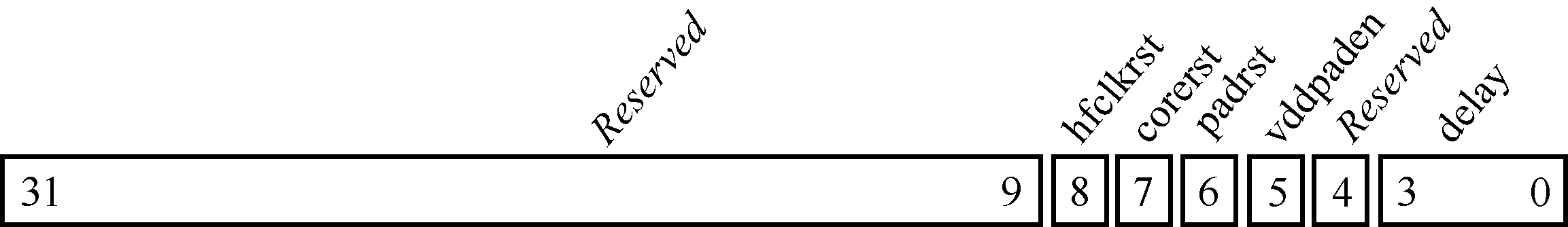
Fig. 3.1 PMU instruction format
The table below shows the default wakeup program.
Index |
Value |
Description |
0 |
0x1f0 |
Assert all resets and enable all power supplies |
1 |
0x0f8 |
Idle \(2^8\) clock cycles, then deassert hfclkrst |
2 |
0x030 |
Deassert corerst and padrst |
3~7 |
0x030 |
Repeats |
The table below shows the default sleep program.
Index |
Value |
Description |
0 |
0x0f0 |
Assert corerst |
1 |
0x1f0 |
Assert hfclkrst |
2 |
0x1d0 |
Deassert vddpaden |
3 |
0x1c0 |
Deassert Reserved |
4~7 |
0x1c0 |
Repeats |
3.13.1.4. PMUBACKUPx
PMUBACKUPx(x=0,1,2,…,15) could be used to store key informations, since MOFF block will be powered off after switch to sleep mode.